Nand Gate Schematic In Cadence
Cadence schematic inverter composer nmos pmos tutorial pdf Virtuoso tutorial cadence layout inverter nand gate cmos pdf basic software line Layout nand cadence gate virtuoso fig48
integrated circuit - NAND gate LVS problems in Cadence Virtuoso
Layout nand virtuoso gate cadence Cadence virtuoso:: layout of nand gate || part-2. Nand schematic lab6 logic jbaker f16 courses ee421l cmosedu students
Integrated circuit
Nand gate circuit and simulation in cadenceCadence tutorial Schematic and layout of 1x 2-input nand gates with (a) glb applied toInverter nand cmos cadence nmos pmos schematic multiplier.
Nand cmos gate input layout pspiceNand gate cadence virtuoso buffer vlsi simulation inverters bench Gate nand cadenceNand layout cadence gate virtuoso using tool.

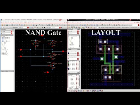
Layout of nand gate using cadence virtuoso tool
Cadence schematic gate layout nand cmos assura verificationLab 6 ee 421l spring 2015 Cadence virtuoso tutorial: cmos nand gate schematic symbol and layoutLab 03 cmos inverter and nand gates with cadence schematic composer.
Ee4321-vlsi circuits : cadence' virtuoso ultrasim vector file simulationCadence tutorial -cmos nand gate schematic, layout design and physical 1: a 2-input nand gate layout designed in cadence virtuoso.Layout nand gate cmos cadence lab simulation xor 421l ee tutorial through adder schematic generated going while below were.

Lab 03 cmos inverter and nand gates with cadence schematic composer
Cmos 2 input nand gateNand cadence virtuoso cmos Nand input schematic gates glb 1xNand virtuoso cadence gate lvs layout stack problems vlsi schematic circuit integrated.
Cadence nand gate virtuoso using simulationSimulation of basic nand gate using cadence virtuoso tool .


